| CPC H04N 25/704 (2023.01) [G06T 5/002 (2013.01); H04N 25/60 (2023.01); G06T 2207/20016 (2013.01)] | 10 Claims |
|
1. An image processing device, comprising:
circuitry configured to:
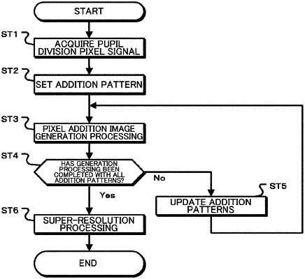
correct pupil division pixel signals of pupil division pixels to correct an inter-pixel sensitivity difference between the pupil division pixels;
add the corrected pupil division pixel signals pupil units of the pupil division pixels with different addition patterns;
generate, based on the added pupil division pixel signals, respective pixel addition images for the different addition patterns; and
generate, based on the generated pixel addition images, an output image with a resolution higher than resolutions of the generated pixel addition images.
|