| CPC H04N 25/633 (2023.01) [H01L 27/14605 (2013.01); H01L 27/14623 (2013.01); H04N 25/75 (2023.01); H10K 30/80 (2023.02); H10K 39/32 (2023.02)] | 20 Claims |
|
1. An imaging device, comprising:
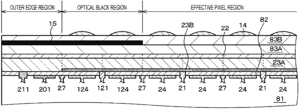
an effective pixel region that includes a plurality of imaging elements-A, amplifies a signal charge generated by photoelectric conversion, and reads the signal charge into a drive circuit; and
an optical black region that includes a plurality of imaging elements-B, surrounds the effective pixel region, and outputs optical black that serves as a reference for black level,
wherein a photoelectric conversion layer forming the plurality of imaging elements-A and the plurality of imaging elements-B is a common photoelectric conversion layer,
wherein the common photoelectric conversion layer is located on an outer side of the optical black region, and extends toward an outer edge region surrounding the optical black region,
wherein an outer edge electrode is disposed in the outer edge region,
wherein a light blocking layer forming the plurality of imaging elements-B is located on the outer side of the optical black region and extends toward the outer edge region,
wherein the common photoelectric conversion layer includes an oxide semiconductor material layer and an organic semiconductor material layer, and
wherein the oxide semiconductor material layer extends in the effective pixel region and the optical black region and not in the outer edge region surrounding the optical black region.
|