US 11,792,541 B2
Solid-state imaging device and method of controlling solid-state imaging device
Taiichiro Watanabe, Kanagawa (JP); Tetsuji Yamaguchi, Kanagawa (JP); Yusuke Sato, Kanagawa (JP); and Fumihiko Koga, Kanagawa (JP)
Assigned to SONY SEMICONDUCTOR SOLUTIONS CORPORATION, Kanagawa (JP)
Filed by SONY SEMICONDUCTOR SOLUTIONS CORPORATION, Kanagawa (JP)
Filed on Sep. 2, 2022, as Appl. No. 17/901,994.
Application 17/901,994 is a continuation of application No. 16/640,479, granted, now 11,445,135, previously published as PCT/JP2018/030106, filed on Aug. 10, 2018.
Claims priority of application No. 2017-167852 (JP), filed on Aug. 31, 2017.
Prior Publication US 2022/0417459 A1, Dec. 29, 2022
This patent is subject to a terminal disclaimer.
Int. Cl. H04N 25/626 (2023.01); H10K 39/32 (2023.01)
CPC H04N 25/626 (2023.01) [H10K 39/32 (2023.02)] 20 Claims
OG exemplary drawing
 
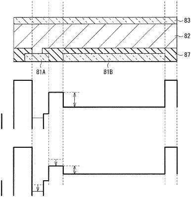
1. A solid-state imaging device, comprising:
a first electrode including a plurality of electrodes, wherein the plurality of electrodes includes a charge readout electrode and an accumulation electrode;
a second electrode opposite to the first electrode;
a photoelectric conversion layer between the first electrode and the second electrode; and
a voltage applier configured to apply different voltages during a charge accumulation period and a charge non-accumulation period to at least one of the first electrode or the second electrode.