| CPC H04N 25/531 (2023.01) [H01L 27/14612 (2013.01); H01L 27/14643 (2013.01); H04N 25/75 (2023.01)] | 20 Claims |
|
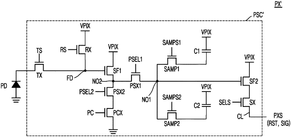
1. An image sensor comprising a plurality of pixels arranged in a plurality of rows and a plurality of columns, each of the plurality of pixels comprising:
a photodiode;
a floating diffusion node configured to accumulate photocharges generated by the photodiode;
a first capacitor configured to store charges according to a voltage of the floating diffusion node which is reset;
a second capacitor configured to store charges according to a voltage of the floating diffusion node in which the photocharges are accumulated;
a first sampling transistor connected to a first output node and configured to sample charges to the first capacitor;
a second sampling transistor connected to the first output node and configured to sample charges to the second capacitor;
a first source follower configured to amplify a voltage of the floating diffusion node and output the amplified voltage to a second output node; and
a precharge transistor having one end connected to the second output node and configured to operate as a current source.
|