| CPC H04B 17/15 (2015.01) [G01R 29/0871 (2013.01); G01R 29/0892 (2013.01); G08B 5/22 (2013.01); H04B 17/23 (2015.01); H04B 17/29 (2015.01); H04B 17/318 (2015.01)] | 18 Claims |
|
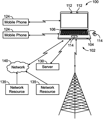
1. An electronic device comprising:
a substrate for receiving communication circuitry;
an antenna coupled to the substrate and configured to provide a first signal to the communication circuitry;
one or more processors;
a data storage device having executable instructions accessible by the one or more processors;
wherein, responsive to execution of the instructions, the one or more processors are configured to:
monitor the antenna or the communication circuitry to detect the first signal;
receive a second signal at the communication circuitry; and
prompt a communication related to the antenna in response to not detecting the first signal when receiving the second signal or detecting a first degraded signal compared to the second signal;
wherein the first signal is the first degraded signal when the first signal has a strength that is less than a threshold percentage of the second signal; and
wherein the threshold percentage varies based on the location of the electronic device or duration of time of monitoring the first signal.
|