US 11,791,887 B2
Communication apparatus and control signal mapping method
Ayako Horiuchi, Kanagawa (JP); Lilei Wang, Beijing (CN); Alexander Golitschek Edler Von Elbwart, Hessen (DE); Hidetoshi Suzuki, Kanagawa (JP); and Kazuki Takeda, Kanagawa (JP)
Assigned to Panasonic Intellectual Property Corporation of America, Torrance, CA (US)
Filed by Panasonic Intellectual Property Corporation of America, Torrance, CA (US)
Filed on Dec. 21, 2022, as Appl. No. 18/69,855.
Application 18/069,855 is a continuation of application No. 17/503,159, filed on Oct. 15, 2021, granted, now 11,569,895.
Application 17/503,159 is a continuation of application No. 17/033,163, filed on Sep. 25, 2020, granted, now 11,177,928, issued on Nov. 16, 2021.
Application 17/033,163 is a continuation of application No. 16/904,291, filed on Jun. 17, 2020, granted, now 10,826,673, issued on Nov. 3, 2020.
Application 16/904,291 is a continuation of application No. 16/681,635, filed on Nov. 12, 2019, granted, now 10,728,010, issued on Jul. 28, 2020.
Application 16/681,635 is a continuation of application No. 16/203,179, filed on Nov. 28, 2018, granted, now 10,505,698, issued on Dec. 10, 2019.
Application 16/203,179 is a continuation of application No. 15/611,394, filed on Jun. 1, 2017, granted, now 10,171,225, issued on Jan. 1, 2019.
Application 15/611,394 is a continuation of application No. 14/781,290, granted, now 9,698,892, issued on Jul. 4, 2017, previously published as PCT/CN2013/073589, filed on Apr. 1, 2013.
Prior Publication US 2023/0130813 A1, Apr. 27, 2023
This patent is subject to a terminal disclaimer.
Int. Cl. H04B 7/08 (2006.01); H04B 7/06 (2006.01); H04W 52/32 (2009.01); H04L 1/00 (2006.01); H04L 5/00 (2006.01); H04L 25/02 (2006.01); H04W 72/23 (2023.01); H04L 27/26 (2006.01); H04B 7/0452 (2017.01)
CPC H04B 7/086 (2013.01) [H04B 7/068 (2013.01); H04B 7/0684 (2013.01); H04B 7/0851 (2013.01); H04L 1/0001 (2013.01); H04L 5/0033 (2013.01); H04L 5/0035 (2013.01); H04L 5/0042 (2013.01); H04L 5/0051 (2013.01); H04L 5/0073 (2013.01); H04L 5/0094 (2013.01); H04L 25/0226 (2013.01); H04L 27/2646 (2013.01); H04W 52/325 (2013.01); H04W 72/23 (2023.01); H04B 7/0452 (2013.01); H04L 1/0003 (2013.01); H04L 1/0009 (2013.01); H04L 5/0007 (2013.01); H04L 5/0026 (2013.01)] 10 Claims
OG exemplary drawing
 
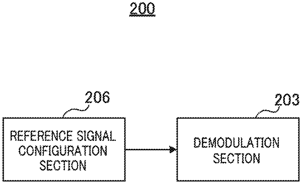
1. An integrated circuit comprising:
reception circuitry, which, in operation, controls receiving a Demodulation Reference Signal (DMRS) and receiving downlink control information indicating a mapping pattern of the DMRS from a plurality of mapping patterns; and
determination circuitry, which, in operation, controls determining the mapping pattern based on the downlink control information,
wherein the plurality of mapping patterns includes a first mapping pattern and a second mapping pattern,
wherein resource elements used for the DMRS of the second mapping pattern are same as a part of resource elements used for the DMRS of the first mapping pattern, and
wherein a number of the resource elements used for the DMRS of the first mapping pattern is larger than a number of the resource elements used for the DMRS of the second mapping pattern.