| CPC H03K 19/017509 (2013.01) [H03K 17/6872 (2013.01)] | 20 Claims |
|
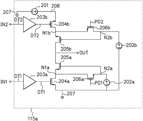
20. A semiconductor integrated circuit, comprising:
an internal circuit configured to output a second input signal; and
a transmission circuit configured to receive the second input signal, wherein
the transmission circuit includes:
a level conversion circuit configured to output a first input signal obtained by performing level conversion on the second input signal, the first input signal having a logic same as that of the second input signal; and
an output circuit configured to receive the first input signal and the second input signal, wherein
the output circuit includes:
a first input transistor of a first conductivity type that is provided between a first power supply line having a first power supply potential and a first intermediate node, and has a gate to which the first input signal is configured to be supplied;
a second input transistor of a second conductivity type that is provided between a second intermediate node and a second power supply line having a second power supply potential, and has a gate to which the second input signal is configured to be supplied;
a first cascode transistor that is provided between the first intermediate node and an output node, and has a gate to which a first clip voltage having an intermediate potential between the first power supply potential and the second power supply potential is configured to be supplied;
a second cascode transistor that is provided between the output node and the second intermediate node, and has a gate to which a second clip voltage having an intermediate potential between the first power supply potential and the second power supply potential is configured to be supplied;
a first switch transistor that is provided between the first intermediate node and the gate of the first cascode transistor, and is configured to turn on during power down;
a second switch transistor that is provided between the second intermediate node and the gate of the second cascode transistor, and is configured to turn on during power down;
a first voltage generation circuit that generates the first clip voltage; and
a second voltage generation circuit that generates the second clip voltage, wherein
the first switch transistor and the second switch transistor are electrically connected via the first voltage generation circuit and the second voltage generation circuit.
|