| CPC H03K 17/063 (2013.01) [H03K 17/08122 (2013.01); H03K 2217/0063 (2013.01); H03K 2217/0072 (2013.01); H03K 2217/0081 (2013.01)] | 20 Claims |
|
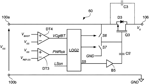
1. A circuit, comprising:
an input supply node;
an intermediate supply node;
a transistor including a bootstrap diode, the transistor having:
a first conduction terminal coupled to the input supply node;
a second conduction terminal coupled to the intermediate supply node; and
a control terminal;
a boosting capacitance having a first side coupled to the control terminal of the transistor and configured to drive the control terminal;
a first switch having a first conduction terminal coupled to the control terminal of the transistor and a second conduction terminal coupled to the first conduction terminal of the transistor; and
a control stage configured to:
in response to determining that a supply voltage of the input supply node is greater than a bootstrap voltage, operate the first switch in a conductive state to short the control terminal to the input supply node; and
in response to determining that the supply voltage is less than a supply voltage threshold, operate the first switch to be in a non-conductive state and the transistor to be in the non-conductive state.
|