| CPC H03K 5/1565 (2013.01) [G11C 7/222 (2013.01); H03K 3/017 (2013.01); H03K 5/135 (2013.01); H03K 2005/00241 (2013.01)] | 11 Claims |
|
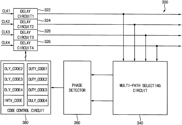
10. A clock error correction device for first, second, third and fourth clock signals having different phases, the clock error correction device comprising:
first, second, third and fourth delay circuits in paths of the first, second, third and fourth clock signals, respectively;
a multi-path selecting circuit configured to output the second clock signal and the first clock signal delayed by a clock interval in a first sub-period of a phase correction period, to output the third clock signal and the second clock signal delayed by the clock interval in a second sub-period of the phase correction period, to output the fourth clock signal and the third clock signal delayed by the clock interval in a third sub-period of the phase correction period, to output the first clock signal and the fourth clock signal delayed by the clock interval in a fourth sub-period of the phase correction period, and to output a first inverted clock signal by inverting the first clock signal and the third clock signal in a duty correction period;
a phase detector configured to compare a rising edge of the second clock signal and a rising edge of the first clock signal delayed by the clock interval in the first sub-period of the phase correction period, to compare a rising edge of the third clock signal and a rising edge of the second clock signal delayed by the clock interval in the second sub-period of the phase correction period, to compare a rising edge of the fourth clock signal and a rising edge of the third clock signal delayed by the clock interval in the third sub-period of the phase correction period, to compare a rising edge of the first clock signal and a rising edge of the fourth clock signal delayed by the clock interval in the fourth sub-period of the phase correction period, and to compare a rising edge of the first inverted clock signal and a rising edge of the third clock signal in the duty correction period; and
a code control circuit configured to store an interval code for the clock interval, to store first, second, third and fourth delay codes for the first, second, third and fourth clock signals, and to store first, second, third and fourth duty codes for the first, second, third and fourth clock signals, to adjust the second delay code in response to the output signal of the phase detector in the first sub-period of the phase correction period, to adjust the third delay code in response to the output signal of the phase detector in the second sub-period of the phase correction period, to adjust the fourth delay code in response to the output signal of the phase detector in the third sub-period of the phase correction period, to adjust the interval code in response to the output signal of the phase detector in the fourth sub-period of the phase correction period, and to adjust the first duty code in response to the output signal of the phase detector in the duty correction period,
wherein each of the first, second, third and fourth delay circuits is configured to adjust a first delay time for both of a rising edge and a falling edge of a corresponding clock signal of the first, second, third and fourth clock signals in response to a corresponding delay code of the first, second, third and fourth delay codes, and is configured to adjust a second delay time for the rising edge, the falling edge, or both of the rising edge and the falling edge of the corresponding clock signal in response to a corresponding duty code of the first, second, third and fourth duty codes, and
wherein the multi-path selecting circuit is configured to adjust the clock interval in response to the interval code.
|