| CPC H03K 3/017 (2013.01) [H02J 7/02 (2013.01); H03K 3/037 (2013.01); H03K 19/20 (2013.01); H02J 50/10 (2016.02)] | 15 Claims |
|
1. A system configured for generating an AC signal having a positive half-cycle and a negative half-cycle, each comprising a plurality of pulse width modulated, PWM, pulses each with an individually designated pulse width, the system comprising:
a first clock circuit configured to provide a first clock signal having a first frequency;
a second clock circuit configured to generate a second clock signal having a second frequency, wherein the second frequency is greater than the first frequency;
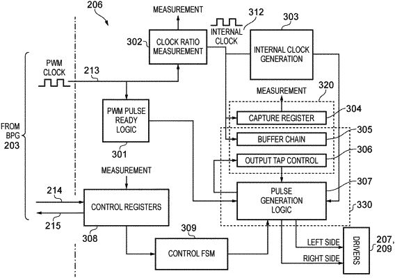
clock ratio measurement circuitry configured to output a first measurement for determining a ratio of the second frequency to the first frequency;
a propagation delay circuit comprising a plurality of propagation delay elements and configured to output a second measurement indicative of a number of propagation delay elements through which a bit transition propagates within a single cycle of the second clock signal;
a pulse data calculation element configured to determine pulse shaping data from the first and second measurements and the individually designated pulse widths; and,
for each of the positive half-cycle and the negative half-cycle, a respective pulse synthesis circuit configured to synthesise the respective plurality of PWM pulses, each PWM pulse of each of the plurality of PWM pulses having a respective start defined by the first clock signal, and a respective pulse width defined by the pulse shaping data and synthesised from the second clock signal and a respective output pulse from the propagation delay circuit.
|