| CPC H03F 3/245 (2013.01) [H03F 1/565 (2013.01); H03F 3/195 (2013.01); H03F 2200/318 (2013.01); H03F 2200/451 (2013.01)] | 20 Claims |
|
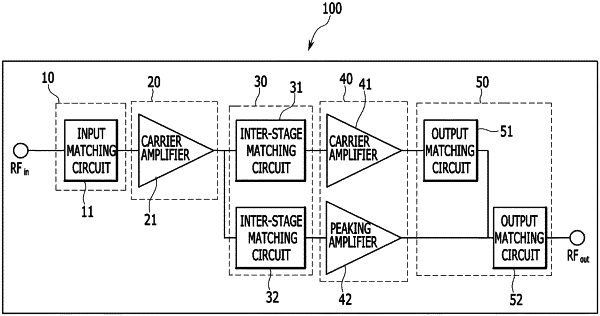
1. A power amplifier system, comprising:
a drive stage configured to amplify an RF input signal and implemented in a substrate containing silicon;
a power stage including a carrier amplifier configured to amplify a base signal from the RF input signal as amplified by the drive stage, and a peaking amplifier configured to amplify a peak signal from the RF input signal as amplified by the drive stage, the power stage being implemented in a substrate containing gallium arsenide; and
a phase compensation circuit configured to change a phase of the RF input signal,
wherein either the carrier amplifier or the peaking amplifier is connected to the phase compensation circuit, and
wherein the carrier amplifier has an operating point in a class B and the peaking amplifier has an operating point in a class C.
|