| CPC H03F 3/193 (2013.01) [G01S 13/08 (2013.01); G01S 13/931 (2013.01); G01S 2013/9314 (2013.01); H03F 2200/451 (2013.01)] | 20 Claims |
|
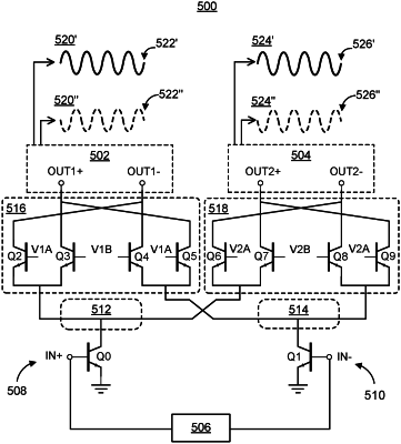
1. A split-steer amplifier with at least one output having an invertible phase, the amplifier comprising:
a first input transistor having its base or gate terminal coupled to a positive node of an input port, its emitter or drain terminal coupled to ground, and its collector or source terminal connected to a positive intermediate node;
a second input transistor having its base or gate terminal coupled to a negative node of the input port, its emitter or drain terminal coupled to ground, and its collector or source terminal connected to a negative intermediate node; and
multiple output ports each having a transistor arrangement that is configured to:
when enabled with a first polarity, couple a positive node of that output port to the positive intermediate node and couples a negative node of that output port to the negative intermediate node;
when enabled with a second polarity, couple the positive node of that output port to the negative intermediate node and couples the negative node of that output port to the positive intermediate node; and
when disabled, decouple the positive node and the negative node of that output port from each of the positive and negative intermediate nodes, wherein the bases or gate terminals of the first and second input transistors being biased to provide quiescent current m*I0 when m of the multiple output ports are enabled, and wherein the enabling of the multiple output ports with the first polarity or the second polarity is associated with an orthogonal phase code that identifies a receive signal corresponding to a receive antenna or identifies a transmit signal corresponding to a transmit antenna.
|