| CPC H02M 1/0054 (2021.05) [H02M 1/08 (2013.01); H02M 3/155 (2013.01)] | 10 Claims |
|
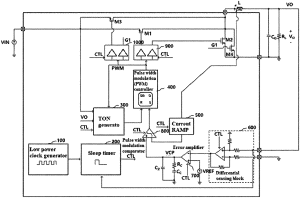
1. A low power control device using a sleep timer, comprising:
a low power clock generator which generates and outputs a clock signal;
the sleep timer which receives the clock signal and an output voltage in a predetermined light load condition to generate a control signal which controls an on/off operation of each component of a circuit;
a TON generator which receives an input voltage, the output voltage, and a reference voltage in response to the control signal to generate a signal for controlling a pulse width modulation;
a pulse width modulation controller which outputs a pulse width modulation signal using an output signal of the TON generator and an output signal of a pulse width modulation comparator;
a current RAMP which receives current information of an inductor provided at an output end of the low power control device in response to the control signal to change the current information into a voltage signal;
a differential sensing block which senses, differentially amplifies, and outputs the output voltage in response to the control signal;
an error amplifier which amplifies an error using the reference voltage and an output signal of the differential sensing block in response to the control signal;
a pulse width modulation comparator which receives an output signal of the error amplifier and an output signal of the current RAMP in response to the control signal to output a comparison signal;
a first gate driver which receives an output signal of the pulse width modulation controller in response to the control signal to output a signal for driving a first power MOSFET; and
a second gate driver which receives an output signal of the pulse width modulation controller in response to the control signal to output a signal for driving a second power MOSFET.
|