| CPC H02J 7/00306 (2020.01) [H01M 10/44 (2013.01); H01M 10/48 (2013.01); H02J 7/0031 (2013.01); H02J 7/0047 (2013.01); H01M 2220/20 (2013.01)] | 7 Claims |
|
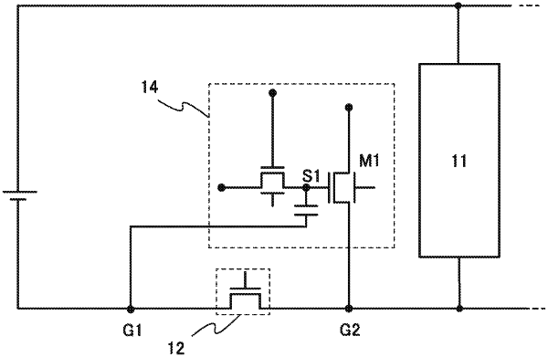
1. An overdischarge prevention circuit of a secondary battery, comprising:
a charging control circuit electrically connected to the secondary battery;
a disconnecting transistor between the secondary battery and the charging control circuit;
a first transistor whose source is electrically connected to a wiring connecting the secondary battery and the disconnecting transistor;
a second transistor connected to a wiring connecting the disconnecting transistor and the charging control circuit; and
a third transistor whose drain or source is connected to a gate of the second transistor.
|