| CPC H01S 5/2275 (2013.01) [H01S 5/0208 (2013.01); H01S 5/04256 (2019.08)] | 11 Claims |
|
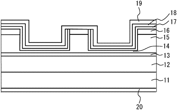
1. A semiconductor laser device manufacturing method comprising:
forming a stacked structure in which a lower cladding layer, an active layer and an upper cladding layer are stacked on an InP substrate in a shape having a mesa stripe structure;
forming a first insulation film on a side face of the mesa stripe structure and lower portions on the left and right of the mesa stripe structure by a sputtering method, the lower portions are lower than the mesa stripe structure;
forming a second insulation film thinner than the first insulation film, on the first insulation film by a plasma CVD method at a film forming temperature higher than that when the first insulation film has been formed; and
forming a first electrode on a top surface of the mesa stripe structure, and forming a second electrode on a back surface of the InP substrate.
|