| CPC H01Q 1/2283 (2013.01) [H01Q 1/52 (2013.01); H05K 1/0242 (2013.01)] | 14 Claims |
|
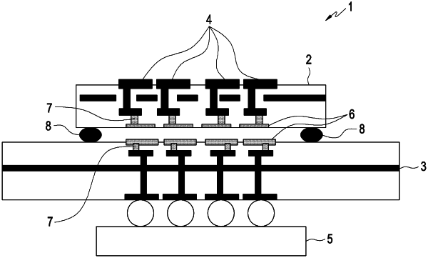
1. A radio frequency (RF) system comprising:
a first RF device and a second RF device separated by a dielectric layer,
each of the first RF device and the second RF device including a plurality of pads disposed on a surface of the device, the pads being surrounded by a common electrode, the common electrode configured as a grounded metal shield,
wherein pads of the first RF device and pads of the second RF device face each other to provide capacitive coupling between the pads and the common electrodes, and
wherein the RF system is configured to transmit signals between the first RF device and the second RF device through the pads.
|