| CPC H01P 3/082 (2013.01) [H01P 3/02 (2013.01); H01P 3/026 (2013.01); H01P 3/06 (2013.01); H01P 3/08 (2013.01); H01P 3/085 (2013.01); H01P 3/088 (2013.01); H05K 1/0245 (2013.01)] | 19 Claims |
|
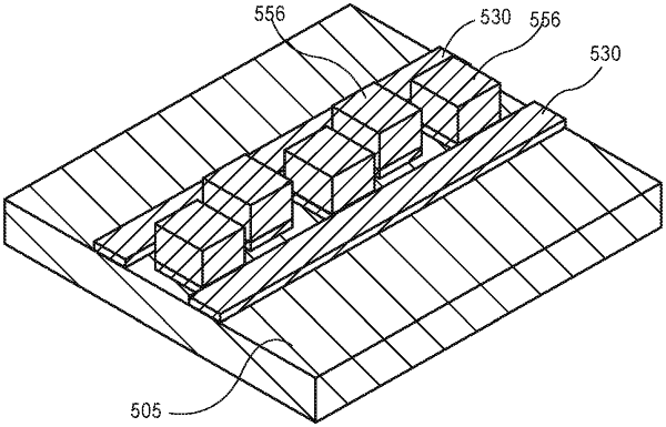
1. A packaged device, comprising:
a stack of dielectric layers;
a first transmission line within the stack of dielectric layers, wherein the first transmission line comprises:
a first linear portion having a first thickness; and
a plurality of first stubs extending out from an edge of the first linear portion, wherein the plurality of first stubs have a second thickness that is greater than the first thickness; and
a second transmission line within the stack of dielectric layers, wherein the second transmission line comprises:
a second linear portion having the first thickness; and
a plurality of second stubs extending out from an edge of the second linear portion, wherein the plurality of second stubs have the second thickness.
|