| CPC H01M 50/534 (2021.01) [C25D 3/12 (2013.01); C25D 7/0614 (2013.01); H01M 10/0525 (2013.01)] | 23 Claims |
|
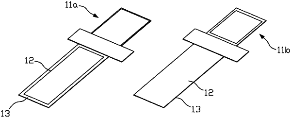
1. A method of manufacturing, comprising:
disposing a tie layer on a second side of a base material, the base material having a first side and the second side;
disposing a first dielectric layer on the tie layer on the second side of the base material;
developing the first dielectric layer on the second side of the base material according to a first pattern;
etching at least a portion of the first side of the base material to form an electrode tab;
micro-etching the tie layer after etching the first side of the base material;
electroplating nickel on the electrode tab; and
applying a second dielectric layer on at least the portion of the first side of the base material that forms the electrode tab.
|