| CPC H01L 33/62 (2013.01) [H01L 24/24 (2013.01); H01L 24/32 (2013.01); H01L 24/73 (2013.01); H01L 25/0753 (2013.01); H01L 33/60 (2013.01); H01L 2224/24011 (2013.01); H01L 2224/24051 (2013.01); H01L 2224/24226 (2013.01); H01L 2224/32057 (2013.01); H01L 2224/32225 (2013.01); H01L 2224/73217 (2013.01)] | 20 Claims |
|
1. A display device comprising:
a first electrode disposed on a substrate;
a second electrode disposed on the substrate and spaced apart from the first electrode;
at least one light-emitting element extending in a second direction, disposed between the first electrode and the second electrode, and electrically connected to the first electrode and the second electrode; and
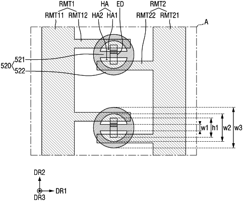
an insulating pattern layer disposed on the first electrode and the second electrode, the insulating pattern layer including:
a fixer disposed directly on at least part of the at least one light-emitting element; and
a barrier surrounding the at least one light-emitting element, the barrier directly contacting the fixer.
|