| CPC H01L 33/62 (2013.01) [H01L 25/0753 (2013.01); H01L 2933/0066 (2013.01)] | 8 Claims |
|
1. A micro device, comprising:
a securing layer;
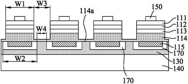
a plurality of micro device units that are separated from each other and that are spaced apart from said securing layer in a laminating direction, each of said micro device units having a plurality of layers disposed on one another along the laminating direction, being surrounded by said securing layer, and cooperating with said securing layer to define a cavity therebetween, the cavity formed squarely between the securing layer and each of the micro device units in a lateral direction or each of the laminating and lateral directions; and
a connecting layer that directly interconnects said micro device units in at least one group of two or more and that is connected to said securing layer so that said micro device units are connected to said securing layer through said connecting layer,
wherein said connecting layer includes a plurality of connecting portions, each of which directly interconnects said micro device units of a respective one of the groups of said micro device units in an extending direction traverse to the laminating direction, each of said connecting portions being formed integrally with and extending from at least one of said layers of each of said micro device units in the respective one of the groups, said connecting layer being made of one of a gallium phosphide based material and a gallium nitride based material, and
wherein said cavities are formed by removing a sacrificial layer in direct contact with said micro device units and said securing layer.
|