| CPC H01L 33/0075 (2013.01) [H01L 21/6835 (2013.01); H01L 33/007 (2013.01); H01L 33/0093 (2020.05); H01L 33/02 (2013.01); H01L 33/06 (2013.01); H01L 33/32 (2013.01); H01S 5/3209 (2013.01); H01S 5/34333 (2013.01); H01L 21/0242 (2013.01); H01L 21/0254 (2013.01); H01L 21/02458 (2013.01); H01L 21/02664 (2013.01); H01L 2221/68368 (2013.01); H01L 2221/68381 (2013.01)] | 20 Claims |
|
1. A method of fabricating a group III nitride heterostructure, the method comprising:
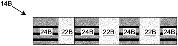
epitaxially growing a sacrificial layer over a substrate structure, wherein the substrate structure includes a substrate and a set of group III nitride layers directly on the substrate, wherein the sacrificial layer is grown directly on a surface of a group III nitride layer in the set of group III nitride layers, wherein each of the set of group III nitride layers in the substrate structure have an aluminum molar fraction of at least 0.5, and wherein the sacrificial layer includes a plurality of sublayers, the plurality of sublayers including: an essentially continuous sublayer and a non-continuous sublayer;
epitaxially growing the group III nitride heterostructure directly on the sacrificial layer; and
decomposing the sacrificial layer by irradiating the sacrificial layer with a laser through the substrate structure to at least partially release the group III nitride heterostructure from the substrate structure, wherein the sacrificial layer is configured to result in absorption of the irradiated laser light at least an order of magnitude higher than any of the set of group III nitride layers in the substrate structure.
|