| CPC H01L 31/107 (2013.01) [H01L 31/03529 (2013.01)] | 20 Claims |
|
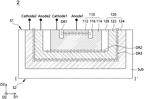
1. A single photon avalanche diode, comprising:
a substrate having an upper surface and a lower surface that are opposite to each other;
a plurality of junction structures formed in the substrate, each of the plurality of junction structures including a first portion exposed to the upper surface of the substrate and a second portion being in contact with an adjacent junction structure; and
an isolation region positioned between first portions of the plurality of junction structures,
wherein each of the plurality of junction structures comprises:
a first impurity region having a first conductive type and corresponding to a part of the first portion that is configured to receive an anode bias; and
a second impurity region having a second conductive type and corresponding to another part of the first portion that is configured to receive a cathode bias, the second impurity region formed to surround the first impurity region and contacting the first impurity region.
|