US 11,791,427 B2
Doped photovoltaic semiconductor layers and methods of making
Sachit Grover, Campbell, CA (US); Stuart Irvine, Denbighshire (GB); Xiaoping Li, Santa Clara, CA (US); Roger Malik, Santa Clara, CA (US); Shahram Seyedmohammadi, Trabuco Canyon, CA (US); Gang Xiong, Santa Clara, CA (US); and Wei Zhang, San Jose, CA (US)
Assigned to First Solar, Inc., Tempe, AZ (US)
Filed by First Solar, Inc., Tempe, AZ (US)
Filed on Oct. 25, 2021, as Appl. No. 17/509,710.
Application 17/509,710 is a continuation of application No. 16/488,275, granted, now 11,158,749, previously published as PCT/US2018/019129, filed on Feb. 22, 2018.
Claims priority of provisional application 62/463,579, filed on Feb. 24, 2017.
Prior Publication US 2022/0045225 A1, Feb. 10, 2022
This patent is subject to a terminal disclaimer.
Int. Cl. H01L 31/0296 (2006.01); H01L 31/18 (2006.01)
CPC H01L 31/02963 (2013.01) [H01L 31/1828 (2013.01); H01L 31/1864 (2013.01)] 16 Claims
OG exemplary drawing
 
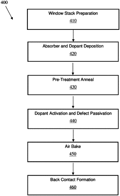
1. A method for treating a photovoltaic semiconductor absorber layer comprising:
supplying a reducing agent to produce a reducing environment;
contacting at least a portion of an absorber layer with a passivating agent while the absorber layer is in the reducing environment, wherein the absorber layer is doped with a group V dopant, and wherein the absorber layer comprises a II-VI semiconductor; and
annealing the absorber layer with the passivating agent while in the reducing environment at a selected temperature and a selected pressure for a selected treatment duration, wherein the reducing environment comprises at least a trace amount of oxygen and a ratio of the partial pressure of the reducing agent to a partial pressure of the oxygen is at least 3.