| CPC H01L 29/7869 (2013.01) [H01L 27/1225 (2013.01); H01L 2924/0002 (2013.01)] | 15 Claims |
|
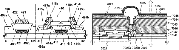
1. A semiconductor device comprising:
a gate electrode layer;
a nitride insulating film over and in direct contact with the gate electrode layer;
an oxide insulating film over and in direct contact with the nitride insulating film;
an oxide semiconductor layer over and in direct contact with the oxide insulating film, the oxide semiconductor layer comprising a channel formation region;
a first insulating layer over and in direct contact with the oxide semiconductor layer;
a first wiring layer in electrical contact with the oxide semiconductor layer;
a second wiring layer over and in contact with the first wiring layer;
a second insulating layer over the first insulating layer;
a third insulating layer over the second insulating layer;
a color filter layer between the second insulating layer and the third insulating layer; and
a first electrode of a light-emitting element over the third insulating layer,
wherein the first wiring layer and the second wiring layer are electrically connected to the oxide semiconductor layer through a first opening of the first insulating layer,
wherein the first electrode of the light-emitting element is electrically connected to the second wiring layer through a second opening of the second insulating layer and a third opening of the third insulating layer,
wherein the channel formation region of the oxide semiconductor layer comprises a crystalline portion,
wherein the oxide semiconductor layer comprises indium, gallium, and zinc,
wherein the first wiring layer comprises molybdenum,
wherein the second wiring layer comprises copper, and
wherein the gate electrode layer is a stacked-layer structure and comprises copper.
|