US 11,791,415 B2
Semiconductor device
Tatsuya Honda, Isehara (JP); Masashi Tsubuku, Atsugi (JP); Yusuke Nonaka, Atsugi (JP); Takashi Shimazu, Nagoya (JP); and Shunpei Yamazaki, Setagaya (JP)
Assigned to Semiconductor Energy Laboratory Co., Ltd., Kanagawa-ken (JP)
Filed by Semiconductor Energy Laboratory Co., Ltd., Atsugi (JP)
Filed on Apr. 13, 2021, as Appl. No. 17/229,021.
Application 17/229,021 is a continuation of application No. 16/812,919, filed on Mar. 9, 2020, granted, now 11,217,701.
Application 16/812,919 is a continuation of application No. 16/381,479, filed on Apr. 11, 2019, granted, now 10,622,485, issued on Apr. 14, 2020.
Application 16/381,479 is a continuation of application No. 15/422,945, filed on Feb. 2, 2017, granted, now 10,290,744, issued on May 14, 2019.
Application 15/422,945 is a continuation of application No. 14/682,356, filed on Apr. 9, 2015, granted, now 9,741,860, issued on Aug. 22, 2017.
Application 14/682,356 is a continuation of application No. 13/626,261, filed on Sep. 25, 2012, granted, now 9,029,852, issued on May 12, 2015.
Claims priority of application No. 2011-215682 (JP), filed on Sep. 29, 2011.
Prior Publication US 2021/0257498 A1, Aug. 19, 2021
Int. Cl. H01L 29/786 (2006.01); H01L 29/04 (2006.01); H01L 29/24 (2006.01); H01L 29/51 (2006.01); G02F 1/1333 (2006.01); G02F 1/1337 (2006.01); G02F 1/1339 (2006.01); G02F 1/1343 (2006.01); H01L 27/12 (2006.01); H01L 29/66 (2006.01); H01L 21/02 (2006.01); H10K 59/121 (2023.01)
CPC H01L 29/7869 (2013.01) [G02F 1/1337 (2013.01); G02F 1/13394 (2013.01); G02F 1/133345 (2013.01); G02F 1/134309 (2013.01); H01L 27/1225 (2013.01); H01L 29/045 (2013.01); H01L 29/24 (2013.01); H01L 29/51 (2013.01); H01L 29/66969 (2013.01); H01L 29/78696 (2013.01); G02F 2202/10 (2013.01); H01L 21/02565 (2013.01); H10K 59/1213 (2023.02)] 10 Claims
OG exemplary drawing
 
1. A semiconductor device comprising:
an oxide semiconductor film over a substrate;
a source electrode and a drain electrode electrically connected to the oxide semiconductor film;
a gate electrode; and
a gate insulating film between the gate electrode and the oxide semiconductor film,
wherein the gate insulating film includes silicon and oxygen,
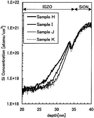
wherein a concentration of silicon in the oxide semiconductor film is lower than or equal to 1.0 at. %,
wherein the oxide semiconductor film includes a region where a concentration of silicon is decreased from an interface with the gate insulating film toward an inside of the oxide semiconductor film, and
wherein the oxide semiconductor film includes a crystal portion.