| CPC H01L 29/7393 (2013.01) [H01L 21/02164 (2013.01); H01L 21/26513 (2013.01); H01L 21/31105 (2013.01); H01L 21/324 (2013.01); H01L 21/76889 (2013.01); H01L 29/0808 (2013.01); H01L 29/45 (2013.01); H01L 29/4916 (2013.01); H01L 29/66325 (2013.01)] | 19 Claims |
|
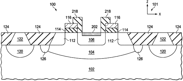
1. A transistor comprising:
a collector region formed over a semiconductor substrate and having majority carriers of a first type, and a collector contact that intersects a top surface of the semiconductor substrate;
a base region formed over the semiconductor substrate and having majority carriers of a second type, the base region having a dopant concentration greater than 1.0*1016 cm−3 at a depth of 0.2 μm, and a base contact that intersects the top surface of the semiconductor substrate;
an emitter region having majority carriers of the first type, the emitter region having a first area and a second area, wherein the base contact surrounds the emitter region and the collector contact surrounds the base contact;
silicide, wherein the silicide is formed in the second area of the emitter region;
a gate oxide over the base region; and
a gate material on the gate oxide, the gate material and the gate oxide having a first sidewall, wherein the silicide formed in the second area of the emitter region is separated from the first sidewall by a distance of at least 0.1 microns.
|