| CPC H01L 29/6656 (2013.01) [H01L 21/02532 (2013.01); H01L 21/02603 (2013.01); H01L 21/02664 (2013.01); H01L 21/30604 (2013.01); H01L 21/76224 (2013.01); H01L 21/823431 (2013.01); H01L 21/823468 (2013.01); H01L 29/0649 (2013.01); H01L 29/0673 (2013.01); H01L 29/42392 (2013.01); H01L 29/66545 (2013.01); H01L 29/66742 (2013.01); H01L 29/78618 (2013.01); H01L 29/78696 (2013.01)] | 18 Claims |
|
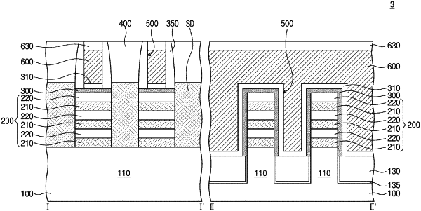
16. A semiconductor device, comprising:
an active pattern protruding from a substrate and including a plurality of stacked semiconductor patterns;
a device isolation pattern provided on a lower portion of the active pattern and exposing an upper portion of the active pattern;
a gate pattern disposed on the active pattern and intersecting the active pattern;
a gate insulating pattern between the gate pattern and the upper portion of the active pattern;
a gate spacer at a side of the gate pattern and on the active pattern;
a capping pattern between the active pattern and the gate spacer;
a source/drain pattern at the side of the gate pattern, the gate spacer disposed between the source/drain pattern and the gate pattern; and
an interlayer insulating layer on an upper surface of the source/drain pattern and on an outer-sidewall of the gate spacer,
wherein the capping pattern is in physical contact with the active pattern,
wherein the capping pattern has a crystalline structure,
wherein the capping pattern has a first sidewall being in physical contact with the gate insulating pattern; and
wherein the capping pattern has a second sidewall being in physical contact with the source/drain pattern and being opposite to the first sidewall.
|