| CPC H01L 29/4966 (2013.01) [H01L 21/28088 (2013.01); H01L 29/66545 (2013.01); H01L 29/66795 (2013.01); H01L 29/7851 (2013.01)] | 20 Claims |
|
1. A manufacturing method of a metal oxide semiconductor field-effect transistor (MOSFET) device, the manufacturing method comprising:
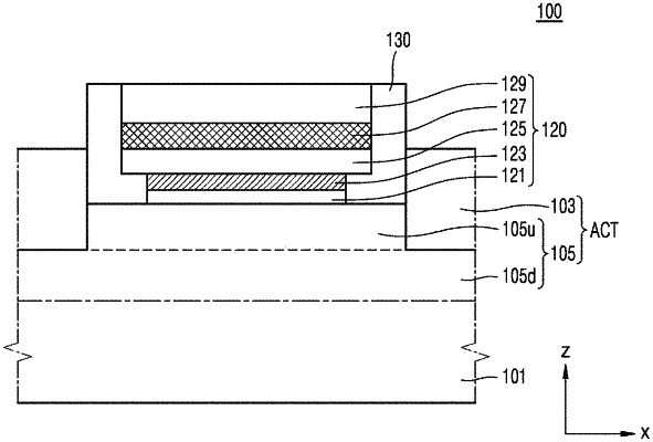
forming an active area having a fin shape, protruding from a semiconductor substrate and extending in a first direction;
forming, on the semiconductor substrate, a dummy gate structure extending in a second direction that traverses the first direction and covering a portion of the active area;
forming two spacers respectively on side surfaces of the dummy gate structure, the side surfaces of the dummy gate structure being spaced apart from each other in the first direction;
removing the dummy gate structure between the two spacers;
forming a high-k layer between the two spacers;
etching inner side surfaces of the two spacers to increase distance between the two spacers;
forming a first metal layer on an upper surface of the high-k layer;
forming a work function control (WFC) layer on the first metal layer; and
forming a second metal layer on the WFC layer,
wherein a lower surface of the WFC layer is longer than a first interface between a lower surface of the first metal layer and the upper surface of the high-k layer in the first direction.
|