| CPC H01L 29/4236 (2013.01) [H01L 21/0217 (2013.01); H01L 21/28088 (2013.01); H01L 21/31056 (2013.01); H01L 21/32136 (2013.01); H01L 21/67075 (2013.01); H01L 29/4238 (2013.01); H01L 29/42368 (2013.01); H01L 29/4966 (2013.01); H01L 29/4991 (2013.01); H10B 12/053 (2023.02); H10B 12/34 (2023.02)] | 15 Claims |
|
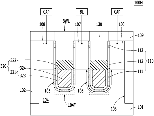
1. A semiconductor device comprising:
a substrate including a trench;
a gate electrode and a capping layer which are sequentially stacked to fill the trench; and
a gate dielectric structure that is conformally formed along a surface of the trench and includes an air gap to partially cover side walls of the gate electrode and side walls of the capping layer,
wherein the gate dielectric structure further includes a first gate dielectric layer and a second gate dielectric layer which are vertically formed with the air gap interposed therebetween.
|