| CPC H01L 29/41775 (2013.01) [H01L 23/66 (2013.01); H01L 29/2003 (2013.01); H01L 29/402 (2013.01); H01L 29/7786 (2013.01); H03F 3/195 (2013.01); H03F 3/213 (2013.01); H01L 2223/6644 (2013.01); H01L 2223/6683 (2013.01); H03F 2200/451 (2013.01)] | 26 Claims |
|
1. A transistor, comprising:
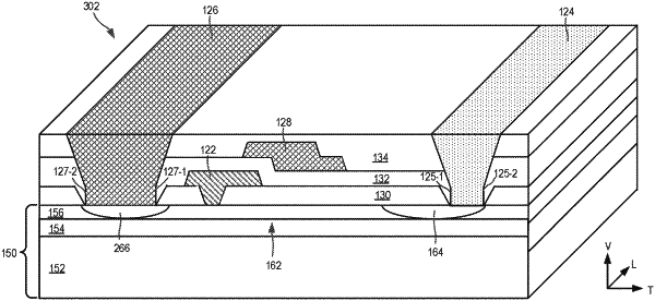
a semiconductor layer structure comprising a gallium nitride-based channel layer and a gallium nitride-based barrier layer that has a higher bandgap than the gallium nitride-based channel layer on an upper surface of the gallium nitride-based channel layer;
a first source/drain region in the semiconductor layer structure;
a second source/drain region in the semiconductor layer structure;
a gate finger on an upper surface of the semiconductor layer structure, the gate finger having a longitudinal axis that extends parallel to the upper surface of the semiconductor layer structure; and
a first source/drain contact on the first source/drain region and a second source/drain contact on the second source/drain region, the first source/drain contact having an inner sidewall that faces the second source/drain contact and an outer sidewall opposite the inner sidewall, and the second source/drain contact having an inner sidewall that faces the first source/drain contact and an outer sidewall opposite the inner sidewall,
wherein the first source/drain region extends a first distance from a lower edge of the inner sidewall of the first source/drain contact towards the second source/drain region along a transverse axis that extends parallel to a plane defined by the upper surface of the semiconductor layer structure, and extends a second distance from a lower edge of the outer sidewall of the first source/drain contact away from the second source/drain region, where the first distance exceeds the second distance,
wherein a location where the first source/drain region has a maximum depth is closer to the lower edge of the inner sidewall of the first source/drain contact than it is to the lower edge of the outer sidewall of the first source/drain contact.
|