| CPC H01L 29/1608 (2013.01) [H01L 29/516 (2013.01); H01L 29/66053 (2013.01); H01L 29/78391 (2014.09)] | 23 Claims |
|
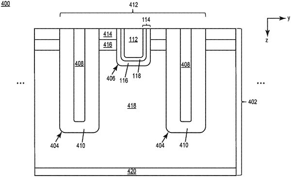
1. A semiconductor device, comprising:
a SiC substrate; and
a plurality of transistor cells formed in the SiC substrate and electrically connected in parallel to form a transistor,
wherein each transistor cell of the plurality of transistor cells comprises a gate structure including a gate electrode and a gate dielectric stack separating the gate electrode from the SiC substrate,
wherein the gate dielectric stack comprises a ferroelectric insulator,
wherein the transistor has a specified operating temperature range,
wherein the ferroelectric insulator is doped with a doping material such that the Curie temperature of the ferroelectric insulator is in a range above the specified operating temperature range of the transistor.
|