| CPC H01L 29/0847 (2013.01) [H01L 27/0886 (2013.01); H01L 29/1608 (2013.01); H01L 29/7854 (2013.01)] | 20 Claims |
|
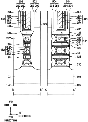
1. A semiconductor device, comprising:
a substrate including a first region and a second region;
first channels on the first region of the substrate, the first channels being spaced apart from each other in a vertical direction perpendicular to an upper surface of the substrate, and each of the first channels extending in a first direction parallel to the upper surface of the substrate;
second channels spaced apart from each other on the second region of the substrate in the vertical direction, each of the second channels extending in the first direction;
a first gate structure extending in a second direction on the first region of the substrate to cover at least a portion of a surface of each of the first channels, the second direction being parallel to the upper surface of the substrate and crossing the first direction;
a second gate structure extending in the second direction on the second region of the substrate to cover at least a portion of a surface of each of the second channels;
a first source/drain layer at each of opposite sides of the first gate structure in the first direction, the first source/drain layer contacting the first channels; and
a second source/drain layer at each of opposite sides of the second gate structure in the first direction, the second source/drain layer contacting the second channels,
wherein:
a first length of a top surface of a third channel among the first channels is greater than a second length of a bottom surface of the third channel, the third channel being an uppermost one of the first channels, and
each of the second channels has a third length in the first direction substantially constant from a top toward a bottom thereof, the third length being greater than the first length.
|