| CPC H01L 29/0634 (2013.01) [H01L 21/047 (2013.01); H01L 29/045 (2013.01); H01L 29/0619 (2013.01); H01L 29/1608 (2013.01); H01L 29/6606 (2013.01); H01L 29/7802 (2013.01); H01L 29/872 (2013.01); H01L 29/0692 (2013.01); H01L 29/1095 (2013.01)] | 18 Claims |
|
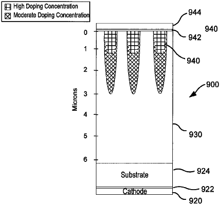
1. A Junction Barrier Schottky (“JBS”) diode, comprising:
a drift region having a first conductivity type; and
a plurality of implanted regions having a second conductivity type in an upper portion of the drift region, where the plurality of implanted regions comprise blocking junctions of the JBS diode,
wherein an upper portion of each of the plurality of implanted regions has a first doping concentration and a lower portion of each of the plurality of implanted regions has a second doping concentration,
wherein the first doping concentration is greater than the second doping concentration, and
wherein the lower portion of each of the plurality of implanted regions is quasi-charge balanced with a respective adjacent portion of the drift region to form a superjunction structure in the drift region.
|