| CPC H01L 29/0626 (2013.01) [H01L 21/8249 (2013.01); H01L 21/823437 (2013.01); H01L 27/0629 (2013.01); H01L 27/0635 (2013.01); H01L 27/088 (2013.01); H01L 29/1083 (2013.01); H01L 29/1087 (2013.01); H01L 29/1095 (2013.01); H01L 29/36 (2013.01); H01L 29/402 (2013.01); H01L 29/42304 (2013.01); H01L 29/4933 (2013.01); H01L 29/66181 (2013.01); H01L 29/66704 (2013.01); H01L 29/7302 (2013.01); H01L 29/735 (2013.01); H01L 29/78 (2013.01); H01L 29/7825 (2013.01); H01L 29/861 (2013.01); H01L 29/8605 (2013.01); H01L 29/872 (2013.01); H01L 29/94 (2013.01); H01L 29/41766 (2013.01); H01L 29/4236 (2013.01); H01L 29/66659 (2013.01); H01L 29/66681 (2013.01); H01L 29/66696 (2013.01); H01L 29/7821 (2013.01); H01L 29/7824 (2013.01); H01L 29/7835 (2013.01); H01L 2224/0401 (2013.01); H01L 2224/05552 (2013.01); H01L 2224/05569 (2013.01); H01L 2224/05572 (2013.01); H01L 2224/11 (2013.01); H01L 2224/13 (2013.01); H01L 2924/00 (2013.01); H01L 2924/00014 (2013.01); H01L 2924/12032 (2013.01); H01L 2924/1305 (2013.01); H01L 2924/13062 (2013.01); H01L 2924/13091 (2013.01)] | 8 Claims |
|
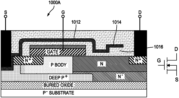
1. A semiconductor structure comprising at least one metal-oxide-semiconductor field-effect transistor (MOSFET) power device, the semiconductor structure comprising:
an active region;
a buried well having a first conductivity type formed in the active region;
a source region having a second conductivity type formed in the active region proximate an upper surface of the active region, the source region being electrically connected to the buried well;
a drain region having the second conductivity type formed in the active region proximate the upper surface of the active region and spaced laterally from the source region;
a body region having the first conductivity type formed in the active region between the source region and the drain region, the body region being formed in direct contact on at least a portion of the buried well;
a gate formed above the active region proximate the upper surface of the active region, wherein the gate is electrically isolated from the active region by a gate insulating layer;
a drain terminal formed on the upper surface of the active region and electrically connected to the drain region;
a source terminal electrically connected to the source region;
a gate terminal electrically connected to the gate; and
a shielding structure formed proximate the upper surface of the active region between the gate and the drain region, wherein the shielding structure comprises a field plate configured to control an electric field distribution along a top oxide interface away from an edge of the gate nearest the drain terminal;
wherein the buried well has a first end below the source terminal and a second end that extends partially below the drain region, the second end being laterally spaced from the drain terminal between the drain terminal and the body region; and
wherein the buried well is configured, in conjunction with the drain region, to form a clamping diode operative to position a breakdown avalanche region between the buried well and the drain terminal.
|