| CPC H01L 28/24 (2013.01) [H01L 21/28531 (2013.01); H01L 27/0676 (2013.01); H01L 27/0682 (2013.01); H01L 27/0794 (2013.01); H01L 27/101 (2013.01); H01L 21/3212 (2013.01)] | 20 Claims |
|
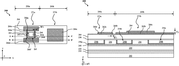
1. A method, comprising:
forming a conductive feature and a first conductive plate over a substrate;
conformally depositing a dielectric layer over the conductive feature and the first conductive plate;
conformally depositing a conductive layer over the conductive feature and the first conductive plate; and
patterning the conductive layer to form a second conductive plate over the first conductive plate and a conductive line extending along a sidewall of the conductive feature.
|