| CPC H01L 27/14656 (2013.01) [H01L 27/14614 (2013.01); H01L 27/14643 (2013.01); H04N 23/75 (2023.01); H04N 25/57 (2023.01); H04N 25/622 (2023.01); H04N 25/76 (2023.01)] | 18 Claims |
|
1. A solid-state imaging device comprising:
a photo diode formed on a substrate;
a floating diffusion which accumulates a signal charge read from the photo diode; and
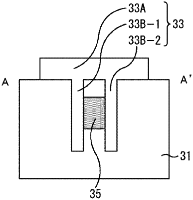
a gate electrode comprising:
a planar gate electrode; and
a plurality of vertical gate electrodes formed from a surface of the substrate in a depth direction in a region between the photo diode and the floating diffusion; and
an overflow path formed in a region interposed between the plurality of vertical gate electrodes, wherein the overflow path is formed in a region shallower than the plurality of vertical gate electrodes.
|