| CPC H01L 27/14645 (2013.01) [H01L 27/14607 (2013.01); H01L 27/14612 (2013.01); H04N 25/59 (2023.01); H04N 25/75 (2023.01); H01L 27/14621 (2013.01); H01L 27/14627 (2013.01)] | 20 Claims |
|
1. An image sensor, comprising:
a pixel array comprising a plurality of detection elements used for both image and focal detection
wherein the plurality of detection elements arrange in a first direction and a second direction,
wherein each of the plurality of detection elements comprises a plurality of photodiodes commonly disposed below a single color filter and divided into a first photodiode group and a second photodiode group, and
at least one of the first photodiode group and the second photodiode group comprises two or more of the plurality of photodiodes being adjacent to one another in at least one of the first direction and the second direction; and
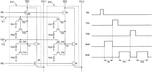
a control logic configured to generate image data by obtaining pixel signals from the plurality of detection elements, and simultaneously read a pixel voltage corresponding to charges generated by two or more of the plurality of photodiodes included in at least one of the first photodiode group and the second photodiode group of one of the plurality of detection elements,
wherein the control logic detects a first pixel voltage corresponding to a charge generated by the first photodiode group by turning on the first transfer transistor, detects a sum pixel voltage corresponding to a sum of charges generated by the first photodiode group and the second photodiode group by turning on the second transfer transistor, and detects a second pixel voltage corresponding to a charge generated by the second photodiode group by calculating a difference between the sum pixel voltage and the first pixel voltage, and
the control logic does not reset a floating diffusion region before detecting the sum pixel voltage after detecting the first pixel voltage.
|