| CPC H01L 27/1463 (2013.01) [H01L 27/14623 (2013.01); H01L 27/14627 (2013.01); H01L 27/14643 (2013.01); H01L 27/14689 (2013.01); H04N 25/75 (2023.01); H04N 25/77 (2023.01); H04N 25/79 (2023.01)] | 17 Claims |
|
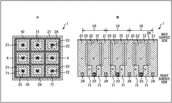
1. A light detecting element comprising:
a substrate; and
a plurality of pixels arranged in a form of a matrix, the plurality of pixels each including:
a first semiconductor layer of a first conductivity type, the first semiconductor layer being formed in an outer peripheral portion in a vicinity of a pixel boundary;
a second semiconductor layer of a second conductivity type opposite from the first conductivity type, the second semiconductor layer being formed on an inside of the first semiconductor layer;
a third semiconductor layer of the second conductivity type on an inside of the second semiconductor layer in a plan view, the third semiconductor layer having a lower impurity concentration than the second semiconductor layer;
a fourth semiconductor layer of low impurity concentration and of the first conductivity type or the second conductivity type, the fourth semiconductor layer being adjacent to the second semiconductor layer in a depth direction of the substrate;
a fifth semiconductor layer of the first conductivity type, the fifth semiconductor layer being adjacent to the second semiconductor layer and being in a front surface of the substrate; and
an on-chip lens (OCL) on a light incident surface.
|