| CPC H01L 27/1463 (2013.01) [H01L 27/1464 (2013.01); H01L 27/14603 (2013.01); H01L 27/14683 (2013.01)] | 20 Claims |
|
1. An image sensor comprising:
a substrate;
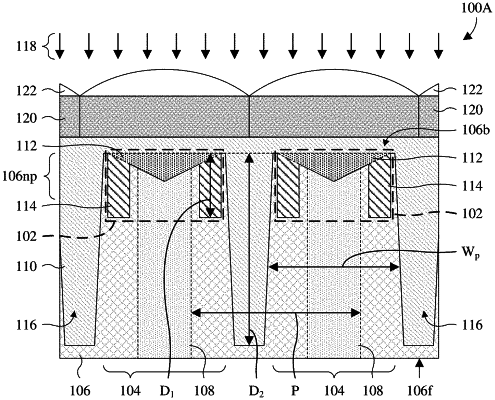
a pixel sensor comprising a photodetector in the substrate;
a first trench isolation structure comprising a pair of first trench isolation segments, wherein the first trench isolation segments are respectively on opposite sides of the pixel sensor at a boundary of the pixel sensor and extend into a backside of the substrate to a first depth;
a second trench isolation structure extending into the backside of the substrate to a second depth less than the first depth between the first trench isolation segments; and
an absorption enhancement structure overlying the photodetector between the first trench isolation segments, wherein the absorption enhancement structure is recessed into the backside of the substrate and has a sidewall directly contacting the second trench isolation structure.
|