| CPC H01L 27/14627 (2013.01) [H01L 27/1463 (2013.01); H01L 27/14607 (2013.01); H01L 27/14685 (2013.01); H01L 27/1462 (2013.01)] | 17 Claims |
|
1. An image sensor, comprising:
a plurality of pixels, each of the pixels including:
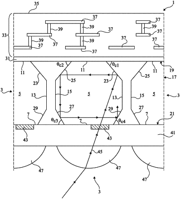
a silicon photoconversion region, the photoconversion region of each pixel extends upwardly from a rear surface to a front surface opposite to the rear surface and extends laterally between four lateral surfaces, the rear surface configured to receive at least one ray, the photoconversion region including:
a first oblique surface coupling a first one of the four lateral surfaces to the front surface;
a second oblique surface coupling the front surface to a second one of the four lateral surfaces opposite to the first lateral surface; and
a third oblique surface coupling the second lateral surface to the rear surface; and
a material at least partially surrounding the photoconversion region, the material having a refraction index smaller than a refraction index of silicon, an interface between the photoconversion region and the material being configured so that the at least one ray reaching the photoconversion region of the pixel undergoes a total reflection or a plurality of successive total reflections at the interface.
|