| CPC H01L 27/14621 (2013.01) [H01L 27/14605 (2013.01); H01L 27/14623 (2013.01); H01L 27/14627 (2013.01); H01L 27/14634 (2013.01); H01L 27/14656 (2013.01); H01L 27/14685 (2013.01)] | 20 Claims |
|
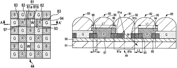
1. An imaging device comprising:
a first pixel configured to receive green light, the first pixel including:
a first photoelectric conversion region,
a first on-chip lens, and
a first light shield disposed between the first photoelectric conversion region and the first on-chip lens, wherein the first photelectric conversion region is overlapped by the first light shield in a plan view;
a second pixel disposed adjacent to the first pixel and configured to receive red light, the second pixel including:
a second photoelectric conversion region,
a second on-chip lens, and
a second light shield disposed between the second photoelectric conversion region and the second on-chip lens, wherein the second photelectric conversion region is overlapped by the second light shield in the plan view; and
a third pixel disposed adjacent to the first pixel and configured to receive white light, the third pixel including:
a third photoelectric conversion region,
a third on-chip lens, and
a third light shield disposed between the third photoelectric conversion region and the third on-chip lens, wherein the third photelectric conversion region is overlapped by the third light shield in the plan view,
wherein an area of the first light shield is less than an area of the third light shield and greater than an area of the second light shield.
|