| CPC H01L 27/1266 (2013.01) [H01L 21/6835 (2013.01); H01L 27/1218 (2013.01); H01L 27/1225 (2013.01); H01L 29/66969 (2013.01); H01L 29/7869 (2013.01); H01L 29/78603 (2013.01); H01L 29/78648 (2013.01); H01L 2221/6835 (2013.01); H01L 2221/68386 (2013.01); H10K 59/1213 (2023.02)] | 6 Claims |
|
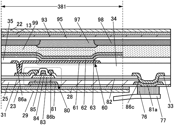
1. A display device comprising:
a first resin layer over a substrate;
a second resin layer over the first resin layer;
a first insulating layer over the second resin layer;
a first gate electrode over the first resin layer;
an oxide semiconductor layer over the first gate electrode;
a gate insulating layer over the oxide semiconductor layer;
a second gate electrode over the gate insulating layer;
a second insulating layer over the oxide semiconductor layer;
a source electrode in contact with the oxide semiconductor layer through a first opening of the second insulating layer;
a drain electrode in contact with the oxide semiconductor layer through a second opening of the second insulating layer;
a third insulating layer over the source electrode and the drain electrode;
a first conductive layer over the third insulating layer, the first conductive layer functioning as a pixel electrode of a light-emitting element;
a fourth insulating layer covering an edge portion of the first conductive layer;
an EL layer of the light-emitting element, over the first conductive layer and the fourth insulating layer;
a second conductive layer of the light-emitting element, over the EL layer;
a third conductive layer over the second insulating layer; and
a fourth conductive layer over the first resin layer, the fourth conductive layer being electrically connected to the third conductive layer,
wherein one of the first opening and the second opening overlaps with the light-emitting element,
wherein the third conductive layer has a region positioned inside a third opening of the second insulating layer, and
wherein the fourth conductive layer has a region in contact with a bottom surface of the third conductive layer.
|