| CPC H01L 27/1225 (2013.01) [G02F 1/1368 (2013.01); H01L 27/1248 (2013.01); H01L 29/401 (2013.01); H01L 29/42384 (2013.01); H10K 59/126 (2023.02); G02F 1/13685 (2021.01); H01L 21/426 (2013.01)] | 5 Claims |
|
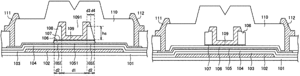
1. Method for manufacturing a display device having a thin film transistor comprising:
a step for forming a first insulating film over a substrate,
a step for forming an oxide semiconductor film over the first insulating film,
a step for patterning the oxide semiconductor film to island shape,
a step for forming a gate insulating film over the oxide semiconductor film and the first insulating film,
a step for forming an aluminum oxide film over the gate insulating film,
a step for forming a gate electrode made of metal,
a step for forming a second insulating film over the oxide semiconductor film and the gate electrode,
a step for forming through holes in the second insulating film, which is an interlayer insulating film, and
a step for forming a drain electrode and source electrode in the through holes to contact the oxide semiconductor film,
wherein the aluminum oxide film over the gate insulating film is removed before the step for forming the second insulating film.
|