| CPC H01L 27/1225 (2013.01) [G02F 1/133345 (2013.01); H01L 21/02565 (2013.01); H01L 27/124 (2013.01); H01L 27/127 (2013.01); H01L 27/1288 (2013.01); H01L 29/66969 (2013.01); H01L 29/7869 (2013.01); H01L 29/78633 (2013.01); H01L 29/78696 (2013.01); G02F 1/1368 (2013.01); G02F 1/13439 (2013.01); G02F 1/13685 (2021.01); G02F 1/136286 (2013.01)] | 20 Claims |
|
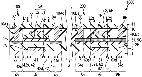
1. An active matrix substrate comprising:
a substrate; and
a plurality of oxide semiconductor TFTs, supported by a principal surface of the substrate, that include a first TFT and a second TFT,
wherein
each of the oxide semiconductor TFTs has an oxide semiconductor layer, a gate insulating layer disposed over a part of the oxide semiconductor layer, a gate electrode disposed over a part of the gate insulating layer, a source electrode, and a drain electrode,
the oxide semiconductor layer of the first TFT is formed from a first oxide semiconductor film,
the oxide semiconductor layer of the second TFT is a layer that is separate from the oxide semiconductor layer of the first TFT, and is formed from a second oxide semiconductor film that is higher in mobility than the first oxide semiconductor film,
each of the oxide semiconductor layers of the first and second TFTs includes
a high-resistance region covered with the gate insulating layer, and
low-resistance regions located on both sides of the high-resistance region and not covered with the gate insulating layer, the low-resistance regions having smaller specific resistance than the high-resistance region,
the high-resistance region includes a channel region overlapping the gate electrode when viewed from an angle parallel with a direction normal to the principal surface of the substrate and offset regions that, when viewed from an angle parallel with the direction normal to the principal surface of the substrate, overlap the gate insulating layer but do not overlap the gate electrode, the offset regions including source-side and drain-side offset regions located on both sides, respectively, of the channel region,
the low-resistance regions include a source contact region electrically connected to the source electrode, a drain contact region placed opposite the source contact region across the high-resistance region and electrically connected to the drain electrode, a source-side interposed region located between the source contact region and the high-resistance region, and a drain-side interposed region located between the drain contact region and the high-resistance region,
the gate insulating layer of the first TFT includes a first insulating film and a second insulating film disposed over the first insulating film,
the gate insulating layer of the second TFT includes the second insulating film but does not include the first insulating film, and
a total length L1 of the offset regions of the first TFT in a channel length direction is greater than a total length L2 of the offset regions of the second TFT in the channel length direction.
|