| CPC H01L 27/1225 (2013.01) [H01L 27/124 (2013.01); H01L 27/1266 (2013.01); H01L 29/045 (2013.01); H01L 29/4908 (2013.01); H01L 29/7869 (2013.01); H01L 29/78648 (2013.01); H10K 59/126 (2023.02); H10K 59/1213 (2023.02)] | 12 Claims |
|
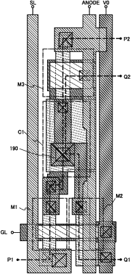
1. A display device comprising a pixel, the pixel comprising:
a light-emitting element;
a first transistor, one of a source and a drain of the first transistor being electrically connected to a pixel electrode of the light-emitting element;
a second transistor, one of a source and a drain of the second transistor being electrically connected to a signal line; and
a third transistor, one of a source and a drain of the third transistor being electrically connected to a wiring,
wherein the other of the source and the drain of the first transistor is electrically connected to a current supply line,
wherein the other of the source and the drain of the second transistor is electrically connected to a gate electrode of the first transistor,
wherein the other of the source and the drain of the third transistor is electrically connected to the pixel electrode,
wherein the display device further comprises:
a first conductive layer functioning as the current supply line;
a second conductive layer functioning as the signal line;
a third conductive layer functioning as the wiring,
a fourth conductive layer electrically connected to the one of the source and the drain of the second transistor;
a fifth conductive layer electrically connected to the other of the source and the drain of the second transistor;
a sixth conductive layer electrically connected to the other of the source and the drain of the third transistor; and
a seventh conductive layer,
wherein the first conductive layer, the second conductive layer, and the seventh conductive layer are positioned in the same layer,
wherein the third conductive layer, the fourth conductive layer, the fifth conductive layer, and the sixth conductive layer are positioned in the same layer,
wherein the first conductive layer and the third conductive layer overlap each other,
wherein the first conductive layer and the gate electrode of the first transistor overlap each other,
wherein the first conductive layer and a gate electrode of the third transistor overlap each other, and
wherein the sixth conductive layer is electrically connected to the pixel electrode through the seventh conductive layer.
|