| CPC H01L 27/1203 (2013.01) [H01L 21/84 (2013.01); H01L 23/528 (2013.01)] | 12 Claims |

|
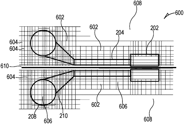
1. A radio-frequency (RF) structure comprising:
a substrate comprising a semiconductor device layer disposed on an insulating layer;
formed in or on the semiconductor device layer, a semiconductor device structure of an integrated RF device; and
disposed above the semiconductor device layer, at least one metallization structure to carry an RF signal to or from the integrated RF device,
wherein the semiconductor device layer, at least over a region that at least partially surrounds the at least one metallization structure, but not in any region in which the semiconductor device structure is formed, comprises implanted ions that increase an electrical resistivity of the semiconductor device layer.
|