| CPC H01L 27/082 (2013.01) [H01L 27/0647 (2013.01); H01L 29/0646 (2013.01); H01L 29/737 (2013.01)] | 12 Claims |
|
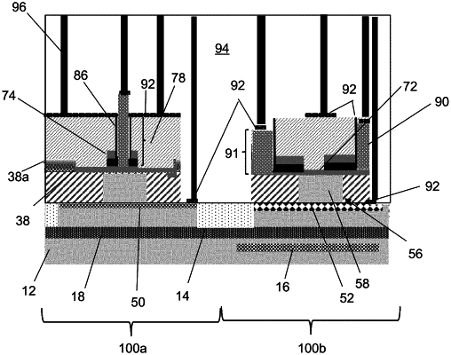
1. A structure comprising:
a first heterojunction bipolar transistor;
a second heterojunction bipolar transistor; and
a trap rich isolation region embedded within a substrate underneath both the first heterojunction bipolar transistor and the second heterojunction bipolar transistor,
wherein the substrate comprises single crystalline semiconductor material and the trap rich isolation region comprises polysilicon crystalline semiconductor material embedded within the single crystalline semiconductor material and further comprising:
a first sub-collector region under a collector region of the first heterojunction bipolar transistor and a second sub-collector region under a collector region of the second heterojunction bipolar transistor, wherein the first sub-collector region and the second sub-collector region are separated from the polysilicon crystalline semiconductor material by an upper portion of the single crystalline semiconductor material and separated from one another by a shallow trench isolation structure; and
a doped isolation region under and separated from the second heterojunction bipolar transistor by a lower portion of the single crystalline semiconductor material ..
|