| CPC H01L 25/18 (2013.01) [H01L 24/08 (2013.01); H01L 24/80 (2013.01); H01L 25/50 (2013.01); H10B 43/10 (2023.02); H10B 43/27 (2023.02); H10B 43/35 (2023.02); H10B 43/40 (2023.02); H10B 43/50 (2023.02); H01L 23/481 (2013.01); H01L 23/5226 (2013.01); H01L 2224/08145 (2013.01); H01L 2224/8083 (2013.01); H01L 2924/1431 (2013.01); H01L 2924/14511 (2013.01); H10B 41/10 (2023.02); H10B 41/27 (2023.02); H10B 41/41 (2023.02)] | 14 Claims |

|
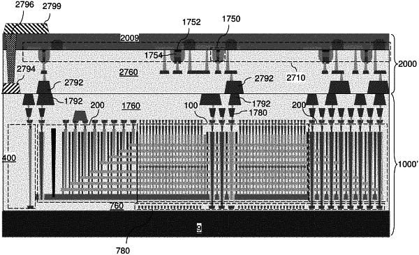
1. A semiconductor structure, comprising:
a first die comprising a three-dimensional memory device including a three-dimensional array of NAND memory elements; and
a second die comprising a semiconductor substrate, a peripheral logic circuitry that includes complementary metal oxide semiconductor (CMOS) devices located on the semiconductor substrate, and a through-substrate via structure that vertically extends through the semiconductor substrate and having a vertical extent that is not less than a thickness of the semiconductor substrate;
wherein:
the first die is bonded to the second die; and
gate structures of the CMOS devices of the second die are located between the three-dimensional array of NAND memory elements of the first die and the semiconductor substrate of the second die containing active regions separated by a channel of the CMOS devices.
|