| CPC H01L 25/18 (2013.01) [H01L 23/49822 (2013.01); H01L 23/5383 (2013.01); H01L 24/16 (2013.01); H01L 2224/16147 (2013.01); H01L 2224/16165 (2013.01)] | 19 Claims |
|
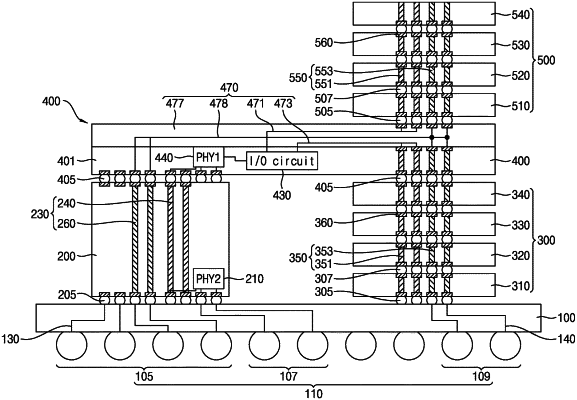
1. A semiconductor package, comprising:
a processor,
a first memory including a plurality of first memory chips;
an interposer disposed over the processor and the first memory; and
a second memory disposed over the interposer, the second memory including a plurality of second memory chips,
wherein the interposer is disposed between the first memory and the second memory,
wherein the interposer comprises a first physical layer (PHY) transmitting and receiving a signal between the processor and the first memory and transmitting and receiving a signal between the processor and the second memory,
wherein the processor comprises a second PHY communicating with the first PHY,
wherein a first through silicon via (TSV) electrically connects the first PHY to the second PHY,
wherein each of the plurality of first memory chips comprises:
a first data TSV receiving a data signal, received from the processor, through the first PHY; and
a first power TSV receiving a power signal from a first substrate, and
wherein each of the plurality of second memory chips comprises:
a second data TSV receiving a data signal, received from the processor, through the first PHY; and
a second power TSV receiving the power signal from the first power TSV.
|