US 11,791,322 B2
Micro LED transfer method and display module manufactured by the same
Doyoung Kwag, Suwon-si (KR); Byungchul Kim, Suwon-si (KR); Eunhye Kim, Suwon-si (KR); Sangmoo Park, Suwon-si (KR); Minsub Oh, Seoul (KR); Dongyeob Lee, Suwon-si (KR); and Yoonsuk Lee, Suwon-si (KR)
Assigned to SAMSUNG ELECTRONICS CO., LTD., Suwon-si (KR)
Filed by SAMSUNG ELECTRONICS CO., LTD., Suwon-si (KR)
Filed on Feb. 22, 2022, as Appl. No. 17/677,182.
Application 17/677,182 is a continuation of application No. 16/866,027, filed on May 4, 2020, granted, now 11,289,462.
Claims priority of application No. 10-2019-0053285 (KR), filed on May 7, 2019.
Prior Publication US 2022/0181311 A1, Jun. 9, 2022
This patent is subject to a terminal disclaimer.
Int. Cl. H01L 25/13 (2006.01); H01L 33/00 (2010.01)
CPC H01L 25/13 (2013.01) [H01L 33/005 (2013.01)] 7 Claims
OG exemplary drawing
 
1. A display module comprising:
a substrate;
a thin film transistor (TFT) layer formed on one surface of the substrate; and
a plurality of light emitting diodes (LEDs) disposed on the TFT layer,
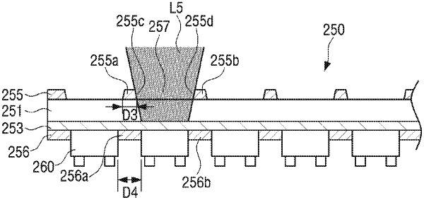
wherein the plurality of LEDs are transferred from a transfer substrate to the TFT layer by a laser beam radiated to the transfer substrate through openings of a mask that is formed integrally with the transfer substrate, and
wherein the openings correspond to regions in which the respective LEDs of the transfer substrate are arranged and the openings correspond to a width, a length, or a unit area of each of the LEDs.